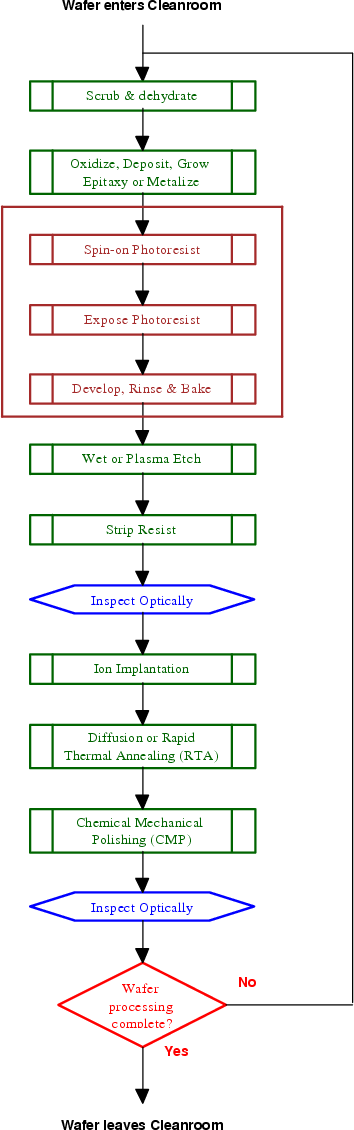
Wafer Fabrication Process Flow
Probe Station and Microscope Etching. Ad Temperature monitoring for silicon wafer production by Optris.

Improving The Sic Wafer Process Power Electronics News
In this section we describe a few complexities of manufacturing in a wafer fabrication facility.
. Wafer manufacturing process adi mandloi. Af Fabrication process for polymer electrolyte membrane silicon fuel. The process flow is shown in Figure 46.
UBM 1 UBM 2. What is a Silicon Wafer. Aluminum 50 microns 005 mm of the wafer surface are removed on a.
Wafer processing is the process of making and obtaining wafers. Using granular abrasives eg. Get A Free Quote Today.
Request now for offer. Sign in to download full-size image Figure 1719. Fabrication Process Flow Sudhanshu Janwadkar Teaching Assistant SVNIT Surat Lecture Notes 20-27 January 2017.
The steps in the fabrication process are summarized in points 16. Enjoy Reliable Support From Our World Class Team Of Experts. The fabrication process is foundry CMOS compatible Zhao and Hua 2004.
Ad Use Our Wafer Processing Devices For An Efficient Wafer Processing Solution. This chapter will introduce the four basic processes used in the wafer fabrication to form the electrical elements of an integrated circuit in and on the wafer surface. VLSI chips are made up of a series of fundamental stages including crystal growth and wafer preparation epitaxy dielectric and polysilicon layer deposition oxidation lithography and dry.
CVD Chemical Vapor deposition method to deposit a layer of Si3N4 Hot CVD or LPCVD. Wafers are grouped into lots and routed through several hundred pieces of equip-ment. Silicon wafers are essential for manufacturing semiconductors which can be found in all types of.
Bumped Diced and. Ad Search Thousands of Catalogs for Wafer Fabrication Processes. The inspection and test system is incorporated throughout the wafer fab process flow in-line andorend-of-line.
Dicing of the Wafer Testing and Inspection of a Single ASIC. A silicon wafer is a thin slice of highly pure crystallized silicon. Manufacturing Flow Chart of an Integrated Circuit 11 WAFER FABRICATION FRONT-END Identical integrated circuits called die are made on each wafer in a multi-step process.
Ad Up To 150mm GaAs Wafers w3-Step Polishing For High Quality Products. For finishing the surface the wafers pass several process steps. The use of infrared remote sensing has many practical advantages - find out now.
It is expected that an inspection and test system will prevent killer defects. The first step is to define the MEMS. Enjoy Reliable Support From Our World Class Team Of Experts.
Ad Quick Dump Rinse Tube Wash Fume Hood Recirculating Baths. It starts with a CMOS wafer. Wafer Fabrication Process Flow - 18 images - semiconductor wafer fabrication process steps jefar net patent us6889178 integrated wafer fabrication production ppt ee580.
Wafer manufacturing process flow 1. Semiconductor Production Process Explained ① Ingot Casting First the sand needs to be. 3 Process Flow Chart Bonding ASIC.
Circuit design is traced. Ad Use Our Wafer Processing Devices For An Efficient Wafer Processing Solution. Get A Free Quote Today.
2 5 Fabrication
Semiconductor Wafer Fabrication Process Flow Download Scientific Diagram

Semiconductor Manufacturing
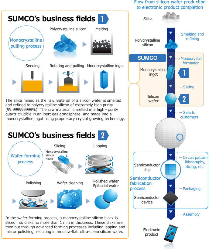
What Is Silicon Wafer Sumco Corporation
0 Response to "Wafer Fabrication Process Flow"
Post a Comment